Advanced PCB layout and
design services
Our PCB layout team has one goal in mind: Get it right the first time.
With an eye on quality, design for manufacturability (DFM), and design for testability (DFT), the DGCD layout design team works hard to accelerate board releases. Our knowledgeable team members use well-tested processes to maintain speed and quality. The team will help with layout designs for:
- New product PCBs – tiny to large, simple to complex
- Product PCB modifications and enhancement
- Obsolescence redesigns
- Quality component footprints and customer libraries
- ASIC and VLSI test boards
DGCD PCB designs include:
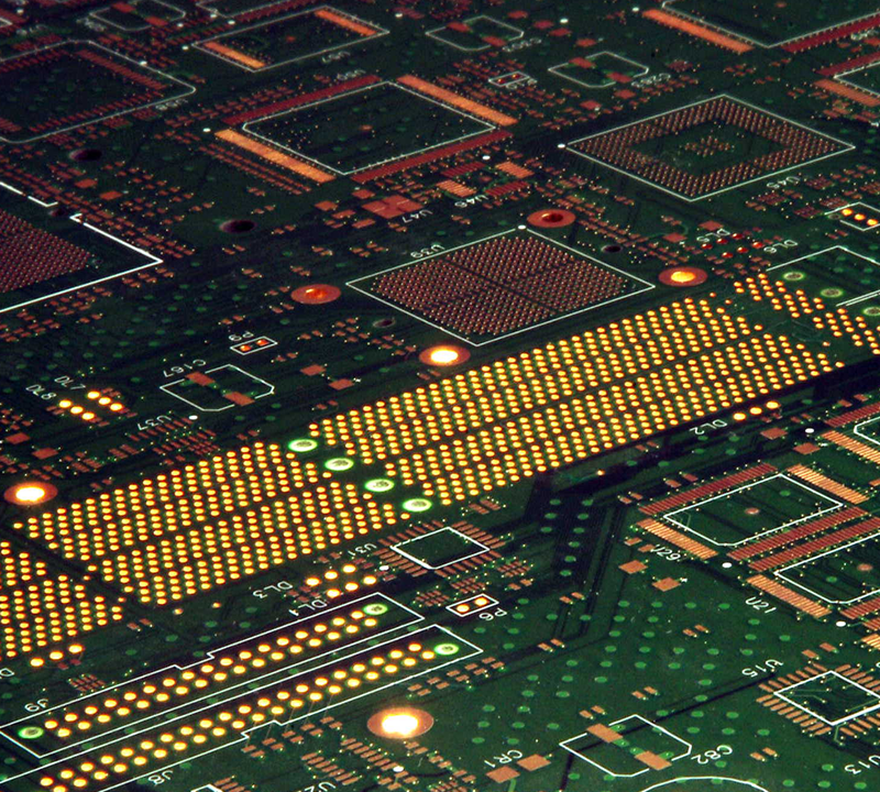
- Single-sided, double-sided, and complex multi-layer boards
- Rigid and flexible circuits
- Microvias – via in pad, blind, buried
- Micro-BGAs and thousand(s) pin BGAs
- Analog, multi-GHz. digital, power, etc.
- Industrial, consumer, aerospace, utilities, etc.
Savvy PCB layout, design, and sourcing saves you money
PCB layout design is at the foundation of the company. In the year 2000, HP’s layout design team launched the company and is still at the heart of the work we do today. Improving PCB layout design is one of the best ways to improve the quality and time to market of electronics products while also reducing production costs. DGCD’s experience and passion for the work will help you achieve the results you need.
DGCD’s expert designers have the advantage of our extensive parts database, plus in-house EE support and procurement support to directly advance the project objectives. Partner with the DGCD team for all your PCB design needs.
Contact us to learn more and get started.
Areas of Expertise:
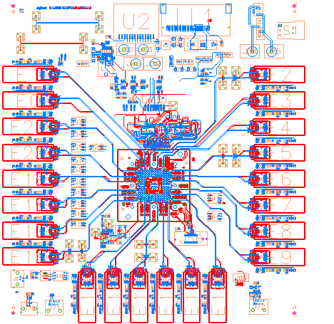
DGCD layout has institutional knowledge that goes back multiple decades and multiple tools. Today we are largely working with Cadence Allegro and the Altium tool set, but we have done designs with Zuken, KiCAD, and Mentor and translated from almost anything out there. The team, with its many years of experience, provides design experience and expertise in many areas and is constantly expanding into the latest protocols, technologies and techniques.
- Memories including DDR4, DDR5, etc.
- Latest bus protocols including PCIe X, USB X, Gig E, etc.
- Aerospace and Class 3 design techniques.
- RF boards and associated techniques.
- Thermal management techniques.
- Complex power planes, pours, splits and isolation.
- Micro BGAs, micro vias, and associated techniques.
- Extensive experience in design rule entry.
- Flex PCB and Rigid Flex PCB designs.
- Board designs with stack-ups to 30+ layers.
- Placement and routing for regulatory compliance.